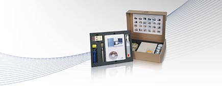
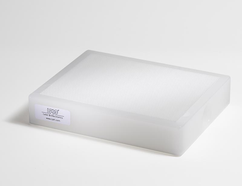
ProConduct
In-House PCB Through-Hole Plating without Chemicals
Revolutionary technology to produce plated through-holes, which does not require a plating tank or potentially hazardous processing chemicals.
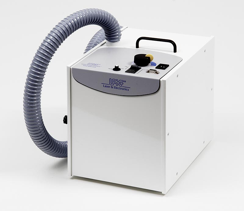
The LPKF ProConduct® through-hole conductivity system creates new technology for producing conductive through-holes without chemical electroplating tanks or potentially hazardous chemical processing.
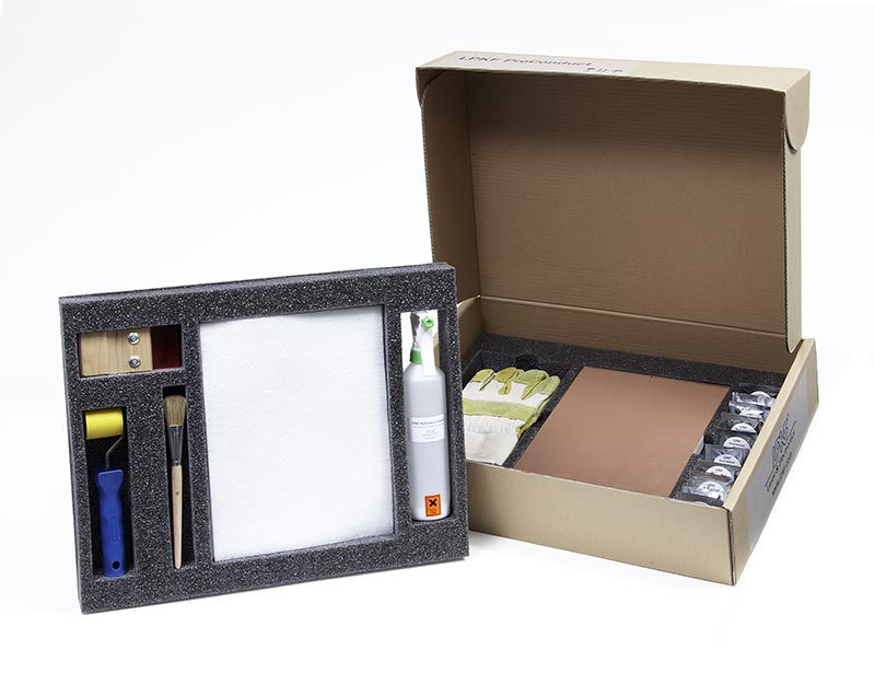
The LPKF ProConduct® system is an ideal solution for many in-house rapid PCB prototyping environments. ProConduct® is perfect for low volume production, laboratories or shops where chemical electroplating is impractical, or any circumstance requiring an economical through-hole conductivity solution. Thanks to a parallel process even boards with high hole count are possible.
Easy to handle
LPKF ProConduct® uses a specially-developed conductive polymer to quickly and easily plate vias in just a few minutes. This four-stop easy-to-learn process lends itself well to parallel processing and results in smoothly plated through-holes in a fraction of the time and cost of chemical electroplating.
Perfect Results
The LPKF ProConduct® system plates vias as small as 0.4mm (15mil) up to an aspect ratio of 1:4. Smaller holes are possible under special conditions. The basic process requires only a few minutes for double-sided and even multilayer boards. The electrical resistance of LPKF ProConduct® results in extremely low – approximately 19.2 mΩ, depending on the material thickness.
Key to in-house work
When combined with LPKF ProtoMat circuit board plotter, the LPKF ProConduct® system becomes a key component to an in-house rapid PCB prototyping solution, featuring security, flexibility, and speed.
1. Mill the board with a LPKF circuit board plotter.

2. Apply special adhesive film to the surface of a milled PCB and drill the through-holes.

Applying the protective film

Drilling the board
3. Apply the conductive polymer to the PCB to fill the through-holes, then use the vacuum table to remove the excess conductor.

Using the squeegee to apply the conductor

Flipping the board
4. Remove the film cure the treated PCB in an oven for about thirty minutes.

Removing the film

Curing the polymer in a hot-air oven
Technical Specifications: ProConduct |
|
| Max. Material Size | 229 mm x 305 mm (9" x 12") |
| Min. Hole Diameter | 0.4 mm (15 mil) up to an aspect ratio of 1:4 |
| Number of Plated Holes | No limit |
| Number of Layers | 4 |
| Solderability | Reflow soldering 250 °C (482 °F), manual soldering 380 °C (716 °F) |
| Base Material Types | FR4, RF- and microwave materials (incl. PTFE-based materials) |
| Processing Time | Approx. 35 min |
| Electric Resistance | Average 19.2 mΩ with standared deviation of 7.7 mΩ |
PDF download
PDF download
PDF download
Which system is best for you?